Semiconductor Electronics: Materials, Devices and Simple Circuits — Important Questions
32 questions
With answersCBSE format
SUMMARY: This chapter covers the principles and applications of semiconductor electronics, including the functioning of various semiconductor devices and their use in simple circuits. KEY TOPICS: intrinsic and extrinsic semiconductors, p-n junction diode, Zener diode, transistors, logic gates, rectifiers, LED, photodiode, solar cell, integrated circuits.
Correct answer: Option 1 — Amplify or switch signals
Short Answer Questions5 questions
Q63 Marks
Distinguish between conductors insulators and semiconductors based on band theory.
View sample solutionHide solution
Conductors (e.g. metals): valence and conduction bands overlap or are partially filled — electrons can flow easily; resistivity ~10⁻⁸ Ω·m. Insulators (e.g. diamond glass): band gap ≥ 3 eV — too large for thermal excitation at room T; very few free electrons; ρ ≥ 10¹² Ω·m. Semiconductors (e.g. Si Ge): band gap ~0.5-1.5 eV — moderate thermal excitation produces some free electrons; ρ ~10⁻³ to 10³ Ω·m at room T; controllable by doping.
Q73 Marks
Distinguish between intrinsic and extrinsic semiconductors.
View sample solutionHide solution
Intrinsic: pure semiconductor with equal numbers of electrons and holes. At room T very few free carriers (n_i ~10¹⁰/cm³ for Si); resistivity is high. Extrinsic: doped semiconductor where impurities (dopants) introduce extra carriers. n-type: pentavalent dopant (P As Sb) provides extra electrons. p-type: trivalent dopant (B Al Ga) provides extra holes. Conductivity of extrinsic semiconductors is many orders of magnitude higher than intrinsic at the same temperature — the basis of all modern electronics.
Q83 Marks
Define depletion region in a pn junction.
View sample solutionHide solution
Depletion region (or depletion layer) is the narrow region around a pn junction where mobile charge carriers (free electrons in n-side and holes in p-side) have diffused and recombined leaving behind ionized donor and acceptor atoms. The result is a region depleted of free carriers and containing fixed charges that produce a built-in electric field opposing further diffusion. Width: typically 0.1-1 μm. Built-in potential: ~0.7 V for Si, ~0.3 V for Ge. Forward bias narrows the region; reverse bias widens it.
Q93 Marks
What is forward and reverse biasing of a pn junction diode?
View sample solutionHide solution
Forward bias: positive terminal of battery connected to p-side and negative to n-side. The applied voltage opposes the built-in potential so the depletion region narrows and current flows easily once V > 0.7 V (for Si). Reverse bias: positive to n-side and negative to p-side. The applied voltage adds to the built-in potential so the depletion region widens and only a tiny reverse saturation current flows. At very high reverse bias the diode breaks down (Zener or avalanche) — used in voltage regulation.
Q103 Marks
Describe how a transistor amplifies a signal.
View sample solutionHide solution
In a common-emitter amplifier (npn transistor): the base-emitter junction is forward biased (low voltage); collector-base junction is reverse biased (high voltage). Small input current at the base controls a much larger collector current — current amplification factor β = I_C/I_B (typically 50-500). A small ac signal at the base produces a much larger ac collector current which when passed through a load resistor produces a much larger ac voltage at the output. Voltage gain A_v = β × R_C/R_in. The transistor acts as a current-controlled current source.
Long Answer Questions5 questions
Q116 Marks
Describe the formation of a pn junction and how it produces a built-in potential.
View sample solutionHide solution
A pn junction is formed by bringing p-type (excess holes) and n-type (excess electrons) semiconductors into contact. Initially: free electrons on the n-side and free holes on the p-side concentration gradient drives diffusion: electrons cross from n to p and holes from p to n. As they cross they leave behind fixed positive ions (donor atoms) on n-side and negative ions (acceptor atoms) on p-side. This creates a built-in electric field directed from n to p that opposes further diffusion. Equilibrium: drift current (due to E) balances diffusion current. The region around the junction depleted of mobile carriers is the depletion region. Built-in potential V_bi = (kT/q) ln(N_A N_D / n_i²) — about 0.7 V for Si.
Q126 Marks
Discuss the working of a half-wave rectifier.
View sample solutionHide solution
A half-wave rectifier consists of one diode and a load resistor connected to a transformer secondary. During the positive half-cycle of input AC the diode is forward biased and conducts — current flows through the load producing positive output voltage. During the negative half-cycle the diode is reverse biased and does not conduct — output is zero. So the output is unidirectional but pulsating: peaks during positive half-cycles zero during negative. Average DC output: V_dc = V_m/π where V_m is peak input. Efficiency: only ~40.6% — half of input cycle is wasted. Used in low-power applications. Full-wave rectifier (using bridge or center-tap configuration) uses both half cycles for higher efficiency (~81%).
Q136 Marks
Discuss the working of an npn transistor as a switch.
View sample solutionHide solution
In switching mode an npn transistor operates in two states: cut-off and saturation. Cut-off (open switch): base-emitter voltage V_BE < 0.7 V → no current flows from base. I_B = I_C = 0. Output (V_CE) is high — connected through R_C to V_CC. The transistor acts as an open switch. Saturation (closed switch): when V_BE = 0.7 V or higher and base current is sufficient (I_B > V_CC/(β × R_C)) → I_C = V_CC/R_C (max possible). V_CE drops to ~0.2 V (saturation voltage). Output is low. The transistor acts like a closed switch. Used in digital circuits LED drivers and relay control. Operating modes: active (analog amplifier) cut-off (off-switch) saturation (on-switch).
Q146 Marks
Calculate the current amplification factor β of a transistor with base current 50 μA and collector current 5 mA. Calculate I_E and α.
View sample solutionHide solution
β = I_C/I_B = (5 × 10⁻³)/(50 × 10⁻⁶) = 5000/50 = 100. Emitter current: I_E = I_C + I_B = 5 mA + 0.05 mA = 5.05 mA. Common-base current gain α = I_C/I_E = 5/5.05 ≈ 0.99. Relation: β = α/(1 − α) = 0.99/0.01 = 99 (approximately matches; small rounding). Typical β values: 50-500 for general-purpose transistors.
Q156 Marks
Discuss the energy band model of semiconductors and explain doping.
View sample solutionHide solution
Energy band model: in a solid the discrete atomic energy levels broaden into bands due to overlap of wavefunctions. Two key bands: valence band (filled with bonding electrons at 0 K) and conduction band (empty at 0 K) separated by a band gap E_g. For pure Si: E_g = 1.12 eV. At 300 K thermal energy kT ≈ 0.026 eV — small fraction of electrons get excited across the gap producing equal numbers of electrons in CB and holes in VB. Doping: replacing a few Si atoms with foreign atoms. n-type: pentavalent (P As) adds extra electron near CB → extra free electrons. p-type: trivalent (B Al) creates a hole near VB → extra holes. Doping increases conductivity by factors of 10⁵ to 10⁹ — transforms a marginally-conducting semiconductor into a useful electronic material.
Assertion–Reason Questions5 questions
Q161 Mark
Assertion (A): Insulators have a large band gap.
Reason (R): A band gap >> kT prevents thermal excitation of electrons from valence to conduction band — almost no free carriers exist.
Show explanationHide explanation
Correct answer: Option 1 —
Both A and R are true, and R is the correct explanation of A.
Q171 Mark
Assertion (A): Doping a semiconductor increases its conductivity significantly.
Reason (R): Dopant atoms introduce charge carriers (extra electrons or holes) that are easily ionized at room temperature.
Show explanationHide explanation
Correct answer: Option 1 —
Both A and R are true, and R is the correct explanation of A.
Q181 Mark
Assertion (A): A pn junction diode conducts well in forward bias.
Reason (R): The applied voltage reduces the built-in potential allowing carriers to flow across the junction.
Show explanationHide explanation
Correct answer: Option 1 —
Both A and R are true, and R is the correct explanation of A.
Q191 Mark
Assertion (A): A transistor can amplify a small signal.
Reason (R): A small base current modulates a much larger collector current due to current gain β.
Show explanationHide explanation
Correct answer: Option 1 —
Both A and R are true, and R is the correct explanation of A.
Q201 Mark
Assertion (A): A half-wave rectifier converts AC to pulsating DC.
Reason (R): The diode conducts only during the half-cycle when it is forward biased blocking the other half-cycle.
Show explanationHide explanation
Correct answer: Option 1 —
Both A and R are true, and R is the correct explanation of A.
Statement-Based Questions5 questions
Q211 Mark
Statement 1: Conductors have very low resistivity.
Statement 2: Insulators have very high resistivity.
Show answerHide answer
Correct answer: Option 1 —
Both statements are true.
Q221 Mark
Statement 1: n-type semiconductors have electrons as majority carriers.
Statement 2: p-type semiconductors have holes as majority carriers.
Show answerHide answer
Correct answer: Option 1 —
Both statements are true.
Q231 Mark
Statement 1: A pn junction conducts well in forward bias.
Statement 2: It blocks current in reverse bias except at breakdown.
Show answerHide answer
Correct answer: Option 1 —
Both statements are true.
Q241 Mark
Statement 1: A transistor can be used as an amplifier or as a switch.
Statement 2: In amplifier mode it operates in the active region.
Show answerHide answer
Correct answer: Option 1 —
Both statements are true.
Statement 2: Modern integrated circuits contain billions of transistors as logic gates.
Show answerHide answer
Correct answer: Option 1 —
Both statements are true.
Case Study / Passage Questions3 questions
Q263 Marks
A student tests a silicon PN junction diode in forward bias. With a 6 V battery and a 1 kΩ series resistor the student observes the diode conducts only when the applied voltage exceeds the cut-in voltage of 0.7 V.
Forward bias means:
AP-region positive
BN-region positive
CBoth positive
DBoth negative
The cut-in (knee) voltage of Si and Ge diodes are:
ASi: 0.7 V Ge: 0.3 V
BSi: 0.3 V Ge: 0.7 V
CSame for both
DZero
Compute the current in this circuit.
Show answersHide answers
1. Option 1 — P-region positive
2. Option 1 — Si: 0.7 V Ge: 0.3 V
3. In forward bias the P-side connects to + and N-side to − terminal — this reduces the depletion region width and lowers the barrier. Once V_applied > V_knee (~0.7 V for Si ~0.3 V for Ge) majority carriers cross the junction in large numbers — diode conducts. Current: I = (V_battery − V_knee)/R = (6 − 0.7)/1000 = 5.3 mA. In reverse bias junction is depleted further blocking majority current — only small reverse saturation current flows.
Q273 Marks
A half-wave rectifier converts 220 V AC (50 Hz) to pulsating DC. A student wants to find the peak DC output frequency of the rectified output and ripple percentage.
The peak voltage of input AC is approximately:
A~110 V
B~155 V
C~220 V
D~311 V
The frequency of the half-wave rectified output is:
A50 Hz
B100 Hz
C150 Hz
D200 Hz
Compare half-wave vs full-wave rectifier.
Show answersHide answers
1. Option 4 — ~311 V
2. Option 1 — 50 Hz
3. Peak voltage: V_peak = √2 × V_rms = √2 × 220 ≈ 311 V. In a half-wave rectifier only the positive half of the AC cycle passes through — output frequency = input frequency = 50 Hz (only positive humps). Average DC: V_DC = V_peak/π ≈ 99 V. Ripple factor: γ = √(I_rms²/I_DC² − 1) ≈ 1.21 for half-wave (very poor) — needs filtering. A full-wave rectifier doubles the output frequency to 100 Hz with ripple factor 0.48.
Q283 Marks
A 5 V Zener diode is used to regulate voltage from a 10 V supply through a series resistor of 100 Ω. A 1 kΩ load is connected across the Zener. A student computes the Zener current.
The Zener current is approximately:
A5 mA
B10 mA
C45 mA
D50 mA
A Zener diode regulates voltage in:
AForward bias
BReverse breakdown
CForward bias
DCut-off
Why does the Zener voltage stay constant?
Show answersHide answers
1. Option 3 — 45 mA
2. Option 2 — Reverse breakdown
3. Output (load) voltage V_L = V_Z = 5 V. Current through R: I_R = (10 − 5)/100 = 50 mA. Current through load: I_L = 5/1000 = 5 mA. Zener current: I_Z = I_R − I_L = 50 − 5 = 45 mA. The Zener operates in reverse breakdown (above the Zener voltage) where it maintains a constant voltage across itself absorbing variations in supply current. Used in power supplies for stable reference voltages and overvoltage protection.
Table-Based Questions3 questions
Q293 Marks
Properties of intrinsic vs. doped semiconductors:
Property
Intrinsic
N-type
P-type
Majority carriers
Equal e and h
Electrons
Holes
Minority carriers
—
Holes
Electrons
Dopant
None
Pentavalent (P As)
Trivalent (B Al)
Conductivity
Low
Higher
Higher
Fermi level
Mid-gap
Closer to CB
Closer to VB
Which is a trivalent dopant for Si?
AP
BSi
CB
DCu
Where is the Fermi level closer to the conduction band?
AHigher in N-type
BHigher in P-type
CSame
DLower in both
How does doping change conductivity?
Show answersHide answers
1. Option 3 — B
2. Option 1 — Higher in N-type
3. Intrinsic Si has only 10¹⁰/cm³ electron-hole pairs at room T. Doping by 1 ppm with phosphorus adds 5 × 10¹⁶/cm³ electrons (since P has 5 valence electrons one extra) — electrons become majority in N-type. Doping with boron creates 'holes' (missing electrons) — holes become majority in P-type. Fermi level shifts according to majority — in N-type close to conduction band in P-type close to valence band. PN junction is formed by combining these two — this is the basis for diodes transistors LEDs solar cells.
Q303 Marks
Diode types and applications:
Diode type
Function
Application
PN junction
Allows one-way current
Rectifiers
Zener
Regulates voltage in reverse
Voltage stabilizer
LED
Emits light when forward biased
Indicator/Display
Photodiode
Generates current under light
Light detector
Solar cell
Converts light to electricity
Solar power
LEDs operate in:
AForward
BReverse
CBoth
DNeither
Which converts solar energy to electricity?
APhotodiode
BSolar cell
CLED
DZener
How does the same PN junction give so many different devices?
Show answersHide answers
1. Option 1 — Forward
2. Option 2 — Solar cell
3. All these devices use the PN junction. Rectifier diodes are forward-biased to allow current — used to convert AC to DC. Zener diodes operate in reverse breakdown — used as voltage references. LEDs use direct-bandgap semiconductors (GaAs InGaN) — electron-hole recombination releases photon E_photon = E_g. Photodiodes and solar cells operate in reverse bias light absorption creates electron-hole pairs that separate at the junction generating current. The same physics — different bias conditions and materials — gives different functions.
Q316 Marks
A silicon PN junction diode has knee voltage 0.7 V and is forward-biased through a 220 Ω resistor by a 5 V battery. In a half-wave rectifier with input V_p = 311 V (50 Hz), with this diode, compute (i) the forward current, (ii) the average DC output voltage assuming ideal diode, (iii) the rectified output frequency, (iv) the ripple factor.
Quantity
Value
Knee voltage
0.7 V
Battery (forward bias)
5 V
Series resistor
220 Ω
AC peak voltage
311 V
AC frequency
50 Hz
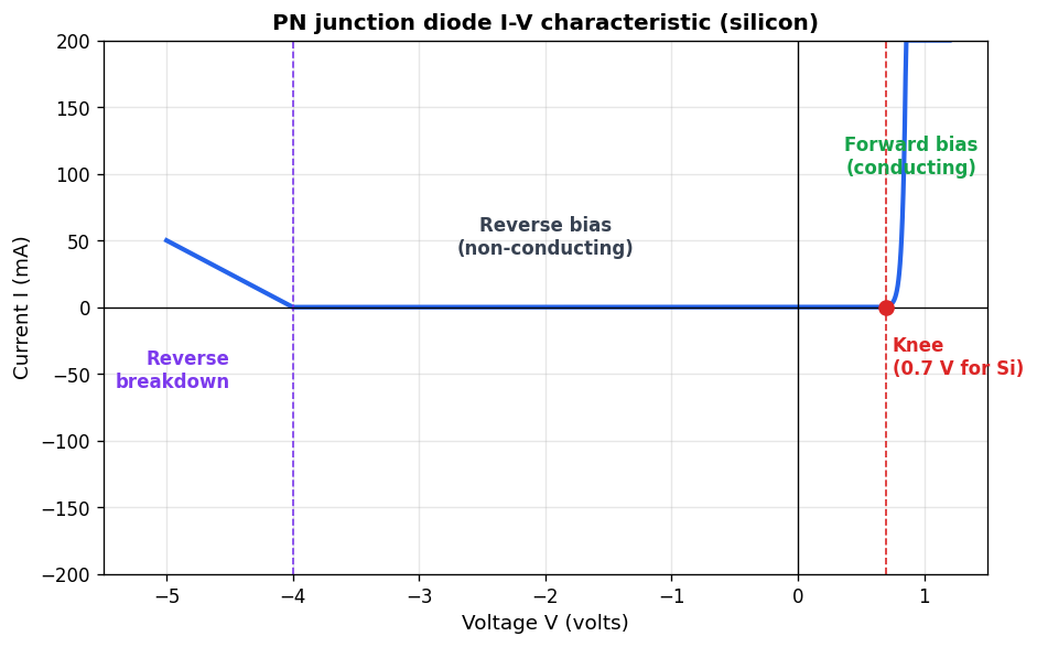
Picture-Based Questions1 question
Q323 Marks
Study the PN junction diode I-V characteristic and answer:
The knee voltage of a silicon PN junction diode is approximately:
A0.3 V
B0.7 V
C1.1 V
D2.0 V
The PN junction diode:
AConducts both ways equally
BConducts only in forward bias
CConducts only in reverse bias
DDoes not conduct at all
Explain the asymmetric I-V characteristic of a PN junction diode.
Show answersHide answers
1. Option 2 — 0.7 V
2. Option 2 — Conducts only in forward bias
3. A PN junction diode is formed by joining a P-type and an N-type semiconductor. In forward bias (P-side connected to + terminal), the depletion region narrows; once the applied voltage exceeds the knee (cut-in) voltage (~0.7 V for Si, ~0.3 V for Ge), majority carriers cross the junction and the current rises rapidly (exponential I-V). In reverse bias, the depletion region widens — only a tiny reverse saturation current flows, of the order of nA-μA. Beyond a certain reverse voltage, the diode undergoes breakdown (Zener or avalanche) — the reverse current rises sharply but the diode is not necessarily damaged (if current is limited by external resistor). This unidirectional conduction is the basis of rectification (AC → DC), used in power supplies, signal demodulation, and protection circuits.